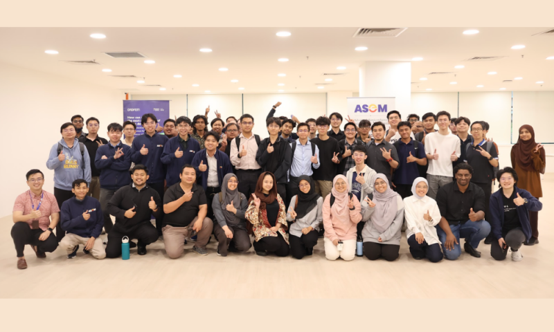
For engineers and startups in Malaysia, bringing a chip from concept to reality has long meant relying on overseas facilities. IC Design Park 2 in Cyberjaya is rewriting that story, offering a homegrown ecosystem where ideas can be designed, tested, and validated under one roof — and where talent meets opportunity.
As Malaysia looks to move beyond contract manufacturing and deepen its role in the global semiconductor value chain, Malaysia Semiconductor IC Design Park 2 represents a strategic shift towards higher-value activities such as IC design, advanced testing, validation, and research. Built as an integrated semiconductor ecosystem, the park combines world-class laboratories, global collaborations, and structured talent development to support local innovation at scale.
A complete laboratory ecosystem
At the core of IC Design Park 2 are four specialised laboratories that collectively support the full lifecycle of semiconductor development — from wafer inspection to advanced research.
1. Advanced Chip Inspection, Test & Metrology Centre (AIM)
Designed for wafer and substrate inspection, AIM ensures high-precision quality control for 6- and 8-inch wafers. Equipped with advanced optical and automation systems, the centre provides detailed measurement, mapping, and defect analysis. Systems like the ISP3100 Optical Inspection System, WID150R Batch Wafer ID Reader, WSS2200 Wafer Sorter, and WIS1000 Optical Inspection System enable fast, accurate, and automated handling of wafers. This allows companies and engineers to maintain consistent quality standards while accelerating testing cycles.

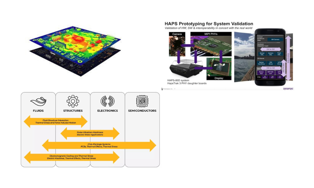
2. Advanced Chip Design, Emulation & Prototype Centre
This lab bridges circuit design and real-world silicon prototypes. Using industry-grade EDA tools, Synopsys HAPS-100 emulators, and Ansys multiphysics simulation software, engineers can design, simulate, and validate analog, digital, and mixed-signal circuits down to 3 nm technology nodes. Enhanced by Tekmark-Keysight instrumentation, including parametric analysers, oscilloscopes, and function generators, the lab enables end-to-end chip design workflows, helping startups and established companies bring innovations from simulation to functional prototypes efficiently.
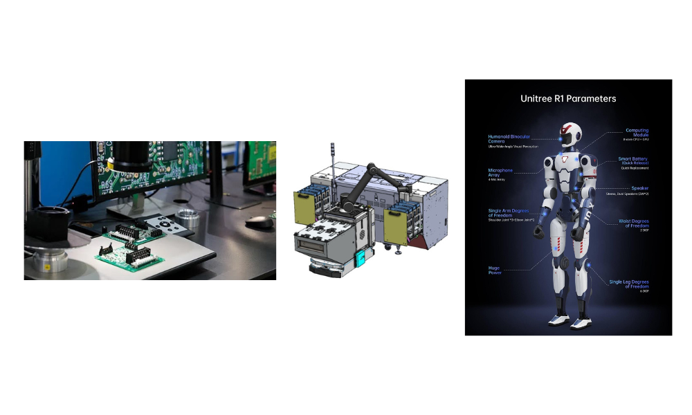
3. Advanced Chip Validation & Robotics Centre
This lab focuses on high-speed chip characterization, debugging, and validation for applications in AI accelerators, automotive electronics, high-frequency communications, and consumer electronics. Precision tools from Tektronix support sub-nanosecond testing to ensure signal integrity, power efficiency, and performance reliability. Robotics integration, featuring DF Automation’s AMRs and the Unitree humanoid robot, enables automated chip handling and adaptive testing, demonstrating the future of human-robot collaboration in semiconductor production.
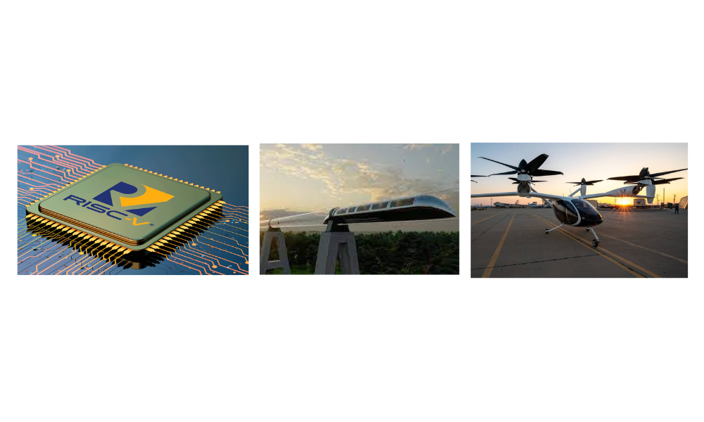
4. Advanced Chip Research & Training Centre
Positioned at the intersection of global IC design hubs in Chennai, Shenzhen, and Hsinchu, this centre drives research and training in advanced semiconductor technologies. Collaborating with IIT Madras Global, Shenzhen Xinhuo Research Centre, Sicada, and Arm, the lab supports deep-tech R&D in AI-integrated systems, power management, mixed-signal design, and next-generation connectivity chips. Its projects span applications from smart devices and automotive systems to aerospace, defense, and industrial automation, fostering innovation across multiple high-impact sectors.
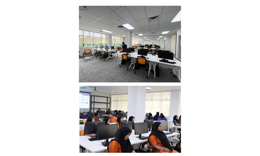
Building talent for the future
A central mission of IC Design Park 2 is human capital development. The Advanced Semiconductor Malaysia Academy (ASEM), housed within the park, aims to train 20,000 semiconductor engineers over the next decade. Purpose-built classrooms, training labs, and collaborative learning spaces within IC Design Park 2 provide an immersive environment where theory meets hands-on practice, enabling engineers to learn directly within an active semiconductor ecosystem. Through intensive, industry-based programs, engineers gain practical experience in IC design, testing automation, and prototype validation — preparing Malaysia’s workforce to meet international standards and support a growing domestic and regional semiconductor ecosystem.
The emphasis on talent reflects a broader national priority. Prime Minister Datuk Seri Anwar Ibrahim has stressed that success in the semiconductor industry depends not only on infrastructure, but on the discipline, adaptability, and depth of knowledge of its people.
“The future belongs to you. Learn as hard as possible and master this discipline because it is changing. You will determine how we can excel as a great nation with digital transformation as our thrust,” he said, addressing students and young engineers preparing to enter the semiconductor field.
IC Design Park 2 is designed to provide the environment where that ambition can be realised — giving local engineers and technologists access to advanced facilities, global expertise, and real-world industry exposure without having to rely on overseas platforms.

Enabling startups and industry collaboration
IC Design Park 2 is not just a research facility — it is a launchpad for startups and industry partnerships. Through the Selangor Semiconductor Fund, Sidec and partners provide strategic investments in promising local startups. Startups gain access to world-class labs, mentorship, and technical expertise, enabling them to accelerate product development and enter global markets.
The park also facilitates collaborations with multinational corporations and international research centres, creating a knowledge-sharing ecosystem where Malaysian engineers and startups can work alongside global industry leaders.
Strategic Location, National Impact
Cyberjaya is more than just a technology hub—it’s where talent, ideas, and innovation naturally come together. Positioning IC Design Park 2 here allows engineers, researchers, startups, and industry players to work side by side, with easy access to universities, research institutions, and technology partners. This close-knit environment shortens the journey from idea to prototype, and from testing to real-world application.
At its core, IC Design Park 2 is about people and possibility. Its integrated ecosystem reduces Malaysia’s reliance on overseas facilities while opening doors to high-value careers and meaningful collaboration. By combining advanced labs, global industry partnerships, and hands-on talent development, the park empowers local innovators to build, test, and scale at home—helping Malaysia move confidently up the global semiconductor value chain while fueling sustainable economic growth and digital innovation.
This content is provided by Sidec
The views expressed here are those of the author/contributor and do not necessarily represent the views of Malaysiakini.
Interested in having your press releases, exclusive interviews, or branded content articles on Malaysiakini? For more information, contact [email protected] or [email protected]